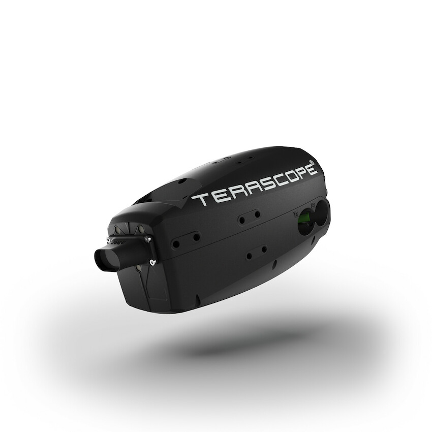


Automated measurement solution for measuring the coating thickness of organic and dielectric single and multilayers as well as performing material analysis using terahertz waves.
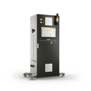
With market-leading precision, repeatability and speed, the innovative TERASCOPE® measurement system is perfectly suited for fully automated inline measuring. Absolutely non-destructive and contactless, the TERASCOPE® penetrates all organic and dielectric materials and can therefore be used for a wide variety of measuring tasks. Its modular design allows system manufacturers and integrators to integrate the measurement system flexibly and individually into their production process.
Up to 6 THz bandwidth* for highest precision and repeatability
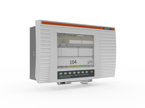
Precise measurement results even in harsh environments thanks to uniquely high sampling rate of 1.6 kHz*
Robust, low-maintenance, developed for 24/7 operation
Less wear and tear due to electro-optical measurement
Continuous dry air purging for unadulterated measurement results
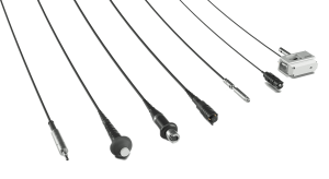
High-precision positioning even on round surfaces and complex geometries
Hardware and software designed for robot and control systems
* Depending on configuration.
Coating thickness measurement of single and multilayer systems including detection of invisible defects and hidden corrosion
Determining of radar transmission and reflection
Coating thickness measurement of single or multilayer systems including detection of invisible defects and inclusions
Testing of material properties
For applications such as wafers and in the fields of biosensor technology, photovoltaics and many more.
Coating thickness measurement of single or multilayer systems including detection of invisible defects and hidden corrosion
Coating thickness measurement of single or multilayer systems including detection of invisible defects
Coating thickness measurement of single or multilayer systems including detection of invisible defects and inclusions
Coating thickness measurement of single or multilayer systems
Testing of material properties
For applications such as wafers and 2D materials (e. g. graphene in photovoltaics), paints, lacquers, and special inks for printing money and many more.